Shifting the Balance of Power
Freescale's low-power technology pushes ahead with Kinetis ARM® Cortex™-M4 MCUs.
Contributed By Convergence Promotions LLC
2011-01-11

The embedded market's demanding appetite for more performance with less power consumption now extends across a wide spectrum of portable and wall-powered applications. To address this demand, Freescale continues to push the boundaries of low-power design. The latest beneficiary is its new Kinetis line of ARM Cortex-M4 microcontrollers. Sampled in the fourth quarter of 2010, Kinetis represents the first broad-market mixed signal MCU portfolio based on the new ARM Cortex-M4 core and one of the most scalable ARM Cortex-M4 MCU portfolios in the industry. Multiple hardware- and software-compatible MCU families will offer exceptional performance, memory and feature scalability ranging from 50 MHz, 32 KB flash devices in ultra-small footprint QFN packages, up to 150 MHz devices with 1 MB of flash memory and rich industrial-focused peripheral sets. Low-power has played a central role in the Kinetis MCU design. This is reflected in the use of Freescale's new 90 nm Split Gate Thin Film Storage (SG-TFS) process technology and in a broad range of general purpose and application specific peripherals that come packed with power-saving functions.
Innovative low-power process technology
Process technology is the basic building block of any semiconductor product and a key factor in determining an MCU's power consumption. Kinetis MCUs are the first to take advantage of Freescale's SG-TFS flash technology which, in addition to offering extremely fast access times and high immunity to charge loss, has been specifically designed to address the needs of power-sensitive applications. In designing the SG-TFS bit cell, Freescale has utilized fast, low voltage transistors in the read path resulting in a lower operating voltage range of 1.71 V to 3.6 V. In applications that utilize two 1.5 V batteries, cell life deteriorates rapidly once the 0.9 V level is reached. This means that the 1.71 V lower voltage limit translates into extended battery life versus traditional MCUs that are typically limited to 2 V or above. This extended voltage range applies not only to the on-chip memories — flash, SRAM and Freescale's new FlexMemory (configurable, high endurance EEPROM) — but also to the analog peripherals, thereby allowing continual signal measuring and conditioning even at the lower end of the power curve. The voltage characteristics of TFS also contribute to reduced run currents by allowing signals that are switched at high speed to operate at lower voltages (typically 1.2 V). Because run current is proportional to C*V^2*f, the reduction in V is very beneficial to the flash component of the active current.
Requisite power modes
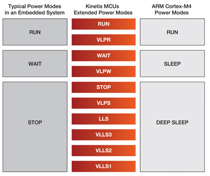
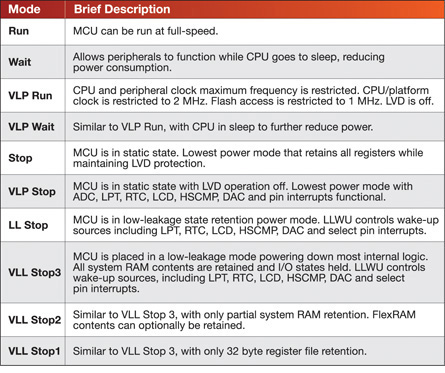
In the majority of battery-operated applications, the CPU spends most of its time in reduced power or sleep modes. It is therefore critical that the MCU offers an attractive selection of power modes, wake-up sources, and start-up times so designers can optimize peripheral activity and recovery times to application requirements and, in turn, extract the most out of the available energy source. Freescale has addressed this by equipping Kinetis MCUs with no less than 10 low-power run, wait and stop modes accompanied by multiple wake-up sources (see Figures 1 and 2). Each run mode comes with a corresponding wait and stop mode. Freescale also has introduced several low-leakage modes and a new low-leakage wake-up controller to satisfy the most aggressive power budgets.


When operating in run mode, the CPU executes code at full speed and can achieve power consumption as low as 200 µA/MHz. For periods when maximum bus frequency is not required, the very low-power run (VLPR) mode can be utilized. This limits the CPU frequency to 2 MHz and places the internal voltage regulator in standby mode while maintaining full peripheral and low voltage detect (LVD) functionality. The power saving achieved in this mode can be significant with VLPR LDD ranging from 600 µA to 1 mA depending on the performance, memory, and peripheral configuration of the MCU.
Wait mode and very low-power wait (VLPW) mode are similar to their equivalent run modes, except that the CPU is halted and flash and FlexMemory programming is unavailable. With peripheral interrupts enabled, the MCU is able to exit wait modes, perform the scheduled task and then quickly revert to a low-power state. This minimizes average power in applications that frequently toggle between active and reduced power states. Depending on the bus frequency, savings of between 30 and 60 percent of the run mode LDD are achievable.
A variety of stop modes provide state retention and partial or full power down of certain logic and/or memory. The low-leakage stop (LLS) mode, the lowest power mode with a 4 µS recovery time, reduces the voltage to internal logic, minimizes leakage from unused internal circuits and has a typical LDD range of 1.2 µA to 7 µA. The very low-leakage stop (VLLS) modes go a step further by powering down the internal logic and optionally the RAM memory, thereby eliminating leakage from unused circuits. The differences between each VLLS mode relate to the level of RAM retention. In VLLS3 mode all RAM is retained; in VLLS2 partial RAM is retained, and in VLLS1 no RAM is retained, but a 32 byte register file is available for storage of critical application data.
A key low-power component of the Kinetis MCU is the low-leakage wake-up unit (LLWU) that acts as the wake-up monitor in all of the low-leakage stop modes. The LLWU supports up to sixteen external input pins (programmable as falling edge, rising edge or any transition) and up to eight internal peripherals that can be configured by the user as wake-up events. In the lowest power mode, several wake-up sources are available: low-power timer, real-time clock, analog comparator, touch-sensing interface (TSI) and several pin interrupts. Wakeup inputs are activated, if enabled, once the MCU enters the LLS mode or any of the VLLS modes.
With clocks consuming as much as 40 percent of active power, Kinetis MCUs employ programmable clock gating for all modules. This shuts down unused peripheral clocks in the run and wait modes while maintaining the same levels of performance and functionality. This is particularly important given the large number of communications modules and timers that are offered on Kinetis devices. Power gating is also employed to shut off inactive memories and logic, further reducing leakage currents.
The Kinetis MCU includes a low-power timer that adds further flexibility by enabling continual system operation in reduced power states. This can be used either as a generic timer or with the on-chip comparators to count comparator output pulses. Finally, a low-voltage detection (LVD) unit supports two low-voltage detection trip points with four warning levels per trip point. It can be configured to generate a reset or interrupt in the event of supply voltage variations, thereby safeguarding memory contents and MCU system states.
Low-power touch sensing
All Kinetis MCUs include Freescale's new Xtrinsic™ touch sense technology. Xtrinsic provides a modern alternative to traditional mechanical pushbutton switches through the creation of touch-activated button, slider, and rotary user interfaces. As well as aesthetic appeal, touch sense interfaces offer design flexibility, low maintenance and the ability to support a variety of sensitivity levels and overlay surfaces. These advantages are driving their adoption beyond the latest consumer gadgets into applications such as home appliances, medical devices and industrial control panels. The touchsense input (TSI) module offers the added benefit of being functional in all low-power modes with only minimal current added when enabled. This opens up touch sensing to a wide range of battery-operated applications that were previously inaccessible.
Within the TSI module is an internal periodic scan unit that has separate scan intervals for low-power and run modes. This allows the user to set long scan intervals for minimizing power consumption. Conversely, in run mode, the scan interval can be reduced for faster touch response.
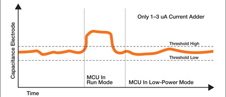
As illustrated in Figure 3, the TSI module has programmable high and low capacitance thresholds within which the CPU remains in sleep mode until a TSI event is detected. When a touch occurs, the instantaneous electrode capacitance is detected to be out of the threshold-defined range, which, in turn, issues a TSI interrupt and quickly wakes up the CPU. Once the touch sense input has been processed, the MCU is then free to return to its reduced power state. The TSI module supports up to 16 electrodes/buttons using a single pin per electrode without the need for external components, enabling reduced system cost. With a capacitance measurement resolution down to 0.02 femto F, it can also be used with thick glass, plastic, and flexi-glass overlays. Furthermore, electrode sampling integration and fault detection hardware increase system robustness, an important consideration in noisy industrial environments.

Several applications require the implementation of keypad, rotary and slider user interfaces. To support this, Freescale offers its Touch Sense Software (TSS) Library which is fully compatible with its CodeWarrior Integrated Development Environment (IDE). Among the features included in the TSS library are smart auto-calibration mechanisms to prevent environmental issues, noise rejection algorithms, an optimized buffer structure that enables any arrangement of electrodes and a PC GUI application for electrode characterization that comes complete with demos and application examples.
Low-power segment LCD
Segment LCD displays are commonly used in a range of power-sensitive applications for providing instructions, monitoring system status, showing operational/functional progress or giving results. In most systems, the LCD is powered at all times, even in reduced power modes, to display status, battery condition, or just time-of-day information. It is therefore essential that the power drawn by the LCD does not adversely affect battery life. The Kinetis K30 and K40 MCU families include a flexible segment LCD controller that supports a wide range of 3 V and 5 V LCD panels with up to 320 segments, and are designed primarily for low-power systems. These MCU families span from 64 KB to 512 KB of flash.
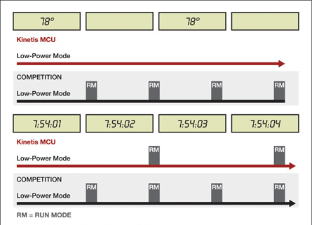
The LCD controller operates in all CPU modes of operation, including very low-leakage stop modes. Unless the chip is in reset, the screen will display information without attention from the rest of the MCU. A key feature is its ability to support blink mode operation, which allows desired segments to be turned on and off at 1/8s, 1/4s, 1/2s, 1s, 2s, 4s, and 8s intervals to either draw attention to that part of the display or simply to conserve power during the 50 percent off cycle. Because blinking is performed in a small part of the LCD module, it, too, runs without having to wake up the CPU, buses or the rest of the MCU. Blinking to a blank screen turns all segments off, while blinking to an alternate screen allows different display data to be shown during the configurable blink period. With this function, the MCU can achieve lower average power consumption by supporting LCD blinking without exiting the low-power mode, as shown in Figure 4.

Minimizing the number of external components also contributes to increased system battery life. The LCD controller generates the frontplane and backplane display signals with a charge pump that requires only four external capacitors.
The data for the LCD is also held at the location closest to the LCD at the pad cell. Rather than LCD data residing in registers deep within the chip, this eliminates the drive necessary to overcome loading between a centralized register and the I/O pins and allows a reduction in the LCD driver voltage domain.
Combined, these low-power features enable consumer, industrial and wireless LCD applications that provide ultra-long life using a variety of batteries, including AA, AAA, lithium coin and 3.6 V. Additional benefits of the LCD controller include the ability to configure any LCD pin as either a frontplane or a backplane via software allowing LCD design changes without the need for costly hardware re-design, segment fault-detection capabilities that guard against erroneous display readouts, and multi-purpose LCD pins that support backplane, frontplane or GPIO functions.
Enabling low-power solutions
With the Kinetis portfolio, Freescale is committed to delivering the latest in low-power MCU innovation. This applies not only to the MCU itself but also to the development tools and design resources that enable it. Kinetis MCUs will be supported by an extensive suite of application notes, reference designs, and training materials. These will be supplemented by a powerful array of third party tools, including IAR Systems Embedded Workbench IDE, which incorporates innovative power debug and analysis tools. These features provide the software developer with the ability to map key events in the program's execution in terms of their power consumption and, in turn, modify their source code to fit their power profile.
Applications today demand more than just low-power. There is frequent need for a broad set of performance, memory, and peripheral options as low-power becomes a critical need on ever-larger numbers of end products. With the industry's latest low-power process technology, multiple low-power operating modes that can be optimized for individual applications, a rich suite of low-power enabled human machine interface peripherals and a comprehensive enablement offering, Kinetis MCUs are ideally positioned to respond. For further information on Kinetis MCUs, visit Freescale's website.

Disclaimer: The opinions, beliefs, and viewpoints expressed by the various authors and/or forum participants on this website do not necessarily reflect the opinions, beliefs, and viewpoints of DigiKey or official policies of DigiKey.


