The Essentials of Analog Voltage Comparators and How to Use Them: Level Detection to Oscillators
Contributed By DigiKey's North American Editors
2020-10-15
As designers look to gather more data at the edge for Internet of Things (IoT), Industrial IoT (IIoT), artificial intelligence (AI), and machine learning (ML) applications, designers need a simple way to detect that a measured value, be it voltage, current, temperature, or pressure, is above or below a threshold. Similarly, it is often necessary to know that a measured quantity is inside or outside of range of values. Making this determination at the edge in the presence of noise and interfering signals is often difficult, but properly selected and applied voltage comparators can help.
A voltage comparator is an electronic device that compares an input voltage with a known reference voltage and changes its output state depending on the whether the input was above or below the reference. This capability satisfies the need to detect threshold crossings, nulls, and signal amplitudes within or outside of an amplitude range.
This article will describe the use of voltage comparators, their characteristics, and the key criteria for their selection. Using example devices from Texas Instruments, the use of voltage comparators for threshold and zero crossing detectors, along with clock recovery and relaxation oscillator applications, will be discussed.
What is a voltage comparator?
A voltage comparator is an electronic device whose output is a logic state that indicates which of its two inputs is at a greater voltage than the other (Figure 1).
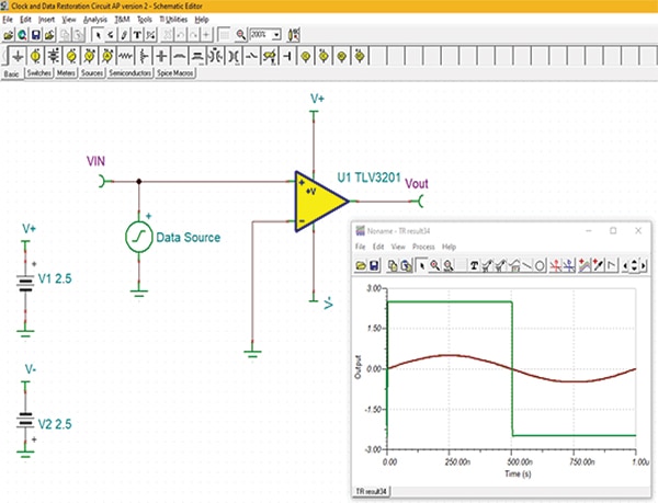 Figure 1: The basic operation of a comparator illustrated in a TINA-TI simulation by applying a sine wave to the non-inverting input of a comparator while the inverting input is referenced to zero volts (ground). (Image source: DigiKey)
The comparator is a Texas Instruments TLV3201AQDCKRQ1 single comparator with push-pull outputs. Like all comparators it has two inputs. An inverting input marked by a minus sign (-), and a non-inverting input marked by a plus sign (+). The comparator inputs are very much like those for an operational amplifier. The main difference is that the comparator output is a digital logic state rather than an analog voltage. In Figure 1 the input is a 1 megahertz (MHz) sine wave with a 200 millivolt (mV) peak amplitude. When the voltage at the non-inverting input is greater than that at the inverting input, the output will be at the high state, 2.5 volts in this case. When the voltage at the non-inverting input is lower than that at the inverting input, the output goes to the low state, -2.5 volts in this case. This comparator has rail-to-rail outputs, so the output logic states extend to the power supply levels. In this example, symmetric positive and negative 2.5 volt supplies are used and are reflected in the output voltage swing.
One way to think about a comparator is that it is a one-bit analog-to-digital converter (ADC). If configured to change state on a zero crossing, its output is essentially a sign bit.
This comparator has a 40 nanosecond (ns) response time, which is specified as the propagation speed or delay. This is the time from the threshold crossing at the input until the output changes state. The propagation speed affects how fast the comparator can switch states, and is in effect, a bandwidth related specification. The TLV3201 also has a built-in voltage hysteresis of 1.2 mV to counter the presence of noise on the signal input.
Hysteresis and noise
If there is noise or spurious signals riding on the comparator input, the threshold may be crossed multiple times and the output may follow the threshold crossings and switch multiple times (Figure 2).
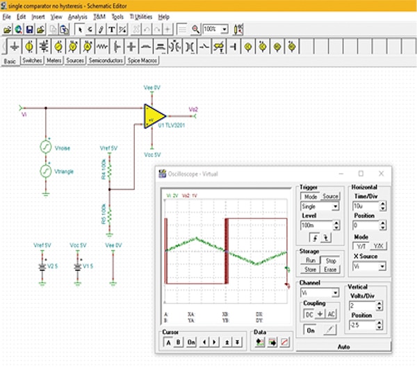 Figure 2: Having noise on the signal input may cause the comparator output to switch multiple times as the noise repeatedly drives the input above and below the threshold. (Image source: DigiKey)
A solution to this unwanted output switching is to add amplitude hysteresis to the comparator circuit. Hysteresis causes the comparator output to hold its state after a threshold crossing until the input amplitude changes by a fixed amount. This is accomplished by applying positive feedback from the output to the input of the comparator which shifts the threshold value by a small increment (Figure 3).
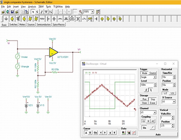 Figure 3: Hysteresis applies positive feedback to the reference input to shift the threshold by a fixed increment. As such, small amplitude changes riding on the input signal cannot change the output. (Image source: DigiKey)
Resistor R3 feeds back the output to the reference input, shifting the reference level a small amount determined by the values of resistors R1, R2, and R3. For the given resistor values, this results in a hysteresis of 400 mV, changing the threshold so that the output state does not change until the input exceeds the hysteresis amplitude. The result is that the output makes a single transition at the threshold crossing.
A few notes about the circuit used compared to the circuit in Figure 1. First, the inverting and non-inverting inputs have been swapped, inverting the output logic. The output is a logic high when the signal is below the threshold. This circuit characteristic is used in circuits that sense when a value is inside or outside a range of values. The TLV3201 is operated with a single five-volt power supply, not the dual 2.5 volt supply used in Figure 1. Because of this, the reference voltage is derived by a voltage divider R1 and R2 to be at 2.5 volts, the common mode voltage for the input. The input signal is also biased to this common mode voltage. The triangle wave has a 2 volt peak amplitude riding on a 2.5 volt bias level. This circuit configuration is a common alternative.
Sensing value inside or outside a window
A single voltage comparator can sense whether an input voltage is above or below a reference threshold value. Determining if an input voltage is between two limits, called windowing, requires two comparators, one for each limit (Figure 4).
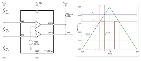 Figure 4: A comparator window circuit configuration uses a dual voltage comparator to determine if the input is within two voltage levels, VL and VH. (Image source: Texas Instruments)
The window circuit shown uses a Texas Instruments TLV6710DDCR dual voltage comparator. The TLV6710 comprises two high accuracy comparators intended for high voltage applications. Supply voltages can be between 1.8 and 36 volts. It includes a 400 mV internal DC reference source. The comparator outputs are open drain connections that can be logically “ORed" by tying them together through a common pullup resistor, as shown. The comparators are wired so that the reference voltage is applied to the inverting input on one (comparator A) and the non-inverting input on the other (comparator B). The input is applied through the voltage divider consisting of resistors R1, R2, and R3 which sets the threshold voltages of 3.3 volts for the lower limit and 4.1 volts for the upper limit. The comparator output is in the high state (3.3 volts) when the input, VMON, is within the window. Comparator A indicates when the input voltage is under 4.1 volts and comparator B shows when the input is over 3.3 volts. Note that both comparators in the TLV6710 have a nominal internal voltage hysteresis of 5.5 mV to help reject noise and small glitches.
The propagation delay of this comparator is typically 9.9 microseconds (µs) for a high-to-low transition and 28.1 µs for a low-to-high transition. This difference is due to the open drain output configuration. The high-to-low transition is an active pulldown by the output FET, while the low-to-high transition is a passive pullup through a resistor which takes more time. This comparator is intended for voltage monitoring applications which do not require an extremely low propagation delay.
Windowing application
Windowing can be used in robotics to control the direction of travel of a robot using light and two CDS photocells. For example, cadmium sulfide (CDS) photocells change their resistance in response to illumination, having a higher resistance when dark and a much lower resistance when illuminated. A TINA-TI simulation illustrates this principle using a Texas Instruments LM393BIPWR dual comparator (Figure 5).
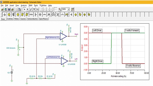 Figure 5: A circuit simulation for a robot steering control using two control motors labelled Left and Right. When 5 volts is applied to the motors they move forward, when 0 volts is applied, they move in reverse. (Image source: DigiKey)
The LM393B comparator is a dual comparator with open-collector outputs that can run on supply voltages from 3 to 36 volts. In this circuit each section provides a motor control signal for each of the two motors designated as left drive or right drive.
A potentiometer is used to model the two CDS photocells. A potentiometer setting from 0% to 40% represents the right photocell being illuminated with the left photocell in the dark. Settings from 60% to 100% signify that light is primarily on the left photocell, with the right photocell dark. From 40% to 60% both photocells are illuminated. When the motor control signal to either motor is at +5 volts the motor turns in the forward direction. If the motor control signal is at 0 volts the motor runs in reverse.
When both photocells are equally illuminated, both motors run in the forward direction, moving the robot straight ahead. When the potentiometer is between 0% and 40%, the left motor runs in the forward direction and the right motor runs in reverse, driving the robot to the right. In the region from 60% to 100% the right motor turns in the forward direction, the left motor is reversed, and the robot turns left.
The comparator reference levels are derived from a voltage divider and are set at 2 volts (40% on the potentiometer) for the right controller and 3 volts (60% on the potentiometer) for the left controller.
Relaxation oscillator
Using both positive and negative feedback, a comparator can be configured as a relaxation oscillator (Figure 6).
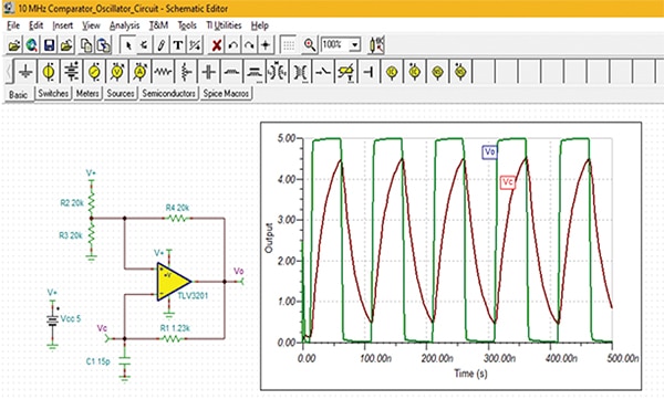 Figure 6: By adding a capacitor to one of the inputs and applying feedback to that capacitor a relaxation oscillator is created. (Image source: DigiKey)
A relaxation oscillator (also called an astable multivibrator) with a square wave output can be created using the circuit shown in Figure 6. The frequency of oscillation is determined by the resistor-capacitor time constant of R1 and C1. With C1 initially discharged (0 volts) the inverting input voltage is below the reference voltage on the non-inverting input. The output is forced to 5 volts. The capacitor C1 is charged via R1 up to the reference voltage at which time the output drops to 0 volts. C1 is discharged through R1 until it falls below the reference voltage and the cycle repeats. The reference voltage has hysteresis (positive) feedback added to it. When the output is 0 volts the reference is 2.5 volts. When the output is 5 volts, the reference voltage increases by about 1.7 volts, bringing it up to 4.2 volts. The transient response, shown in the graph, shows both the output (Vo) and capacitor (Vc) voltage waveforms.
The maximum oscillation frequency is limited by the propagation delay of the comparator. In this case, the Texas Instruments TLV3201 with a 40 ns propagation delay is used to create a 10 MHz oscillator. This frequency is quite close to the maximum for this comparator.
Clock recovery and restoration
Clock signals transmitted through backplanes and cables suffer degradation caused by bandwidth limitations, inter-symbol interference (ISI), noise, reflections, and crosstalk. Comparators can be used to recover clock signals and restore them to a more clearly defined form (Figure 7).
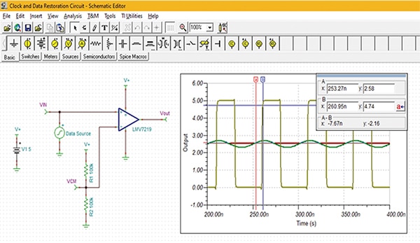 Figure 7: A comparator with a 7 ns propagation delay with internal hysteresis is used to restore a 20 MHz clock. (Image source: DigiKey)
In this type of application, the propagation delay is more critical. The maximum frequency a comparator can track is a function of the propagation delays and output transition times:
![]() Equation 1
Equation 1
Where: fMAX is the maximum toggle frequency
tRise is the output rise time
tFall is the output fall time
tPD LH is the propagation delay from low to high
tPD HL is the propagation delay from high to low
The Texas Instruments LMV7219M5X-NOPB operating with a 5 volt supply has a 1.3 ns rise time, a 1.25 ns fall time, and a typical propagation delay of 7 ns for both transition directions. This yields a maximum toggle frequency of 60.4 MHz. Even with a 2.7 volt supply and longer propagation delay and transition times, the maximum toggle for this comparator rate is about 35 MHz, more than adequate for this 20 MHz clock.
In addition to the remarkably low propagation delay, the LMV7219 incorporates a rail-to-rail push-pull output stage which means short and uniform rise and fall times. It also has internal hysteresis of 7.5 mV to minimize the effects of noise.
Conclusion
Bridging the analog and digital worlds, the voltage comparator is a particularly useful tool, be it for signal levels and windowing for the IIoT, AI, or ML at the edge, or for null detection, clock recovery, or as an oscillator.

Disclaimer: The opinions, beliefs, and viewpoints expressed by the various authors and/or forum participants on this website do not necessarily reflect the opinions, beliefs, and viewpoints of DigiKey or official policies of DigiKey.


